 Xem Studiomeasured geometry
Library › Computers & desk › Keyboard switches & stabilizers ·
Kailh Choc v1 and v2 (PG1350 / PG1353): PCB footprint
Where are the PCB holes for Kailh Choc v1 and v2 low-profile switches? · Standard part · basis: Kailh drawings CPG135001D01 (PG1350, PCB hole drawing) and CPG135301D01 (PG1353, Recommended PCB Layout)
Also called: kailh choc footprint, choc v1 footprint, choc v2 footprint, pg1350 pcb layout, pg1353 pcb layout, choc switch holes, low profile switch footprint, choc v1 v2 compatible pcb, choc plate cutout, choc switch dimensions
Exact dimensions. True size, with no printing tolerance added.
- sizes
- 15 in table
Notes
- Kailh's low-profile Choc switches: v1 (PG1350) has its own two-leg keycap stem; v2 (PG1353) has an MX-style '+' stem. Both put the two contact pins in the same place, so one PCB can take either (and the same Choc hot-swap socket).
- Coordinates are in Kailh's own PCB-layout view, which looks at the copper (solder) side: origin on the switch axis, x to the right, y up. The v1 drawing is turned 180° here so both versions share one orientation; nothing else is changed. For a keycap-side view, mirror left to right (x → −x).
- Differences: the centre hole is Ø3.40 on v1 and Ø5.00 on v2; v1 has two Ø1.90 guide posts on the centre line 11.00 mm apart, v2 has one Ø1.60 guide post at (−5.15, −5.00). A v1+v2 board needs the Ø5.00 centre and all three guide holes.
- Plate: Kailh gives the housing below the top rim (13.80 square on v1, 13.95 ± 0.05 on v2), not a plate cutout or plate thickness, so Xem publishes no plate file; the cutout must clear that housing.
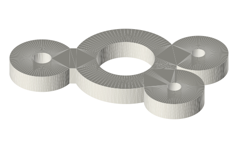
- The files are drill jigs at true size: a ring around every hole joined by bars to the centre hole, to print and drill through or to import as the exact hole pattern. Holes are drawn at the maker's diameters; add your own process allowance.
Kailh Choc v1 and v2 (PG1350 / PG1353): PCB footprint size chart
| parameter | value |
|---|---|
| v1 centre post | Ø3.40 at (+0.00, +0.00) mm |
| v1 contact pin | Ø1.20 at (+5.90, +0.00) mm |
| v1 contact pin | Ø1.20 at (+3.80, +5.00) mm |
| v1 guide post | Ø1.90 at (+0.00, +5.50) mm |
| v1 guide post | Ø1.90 at (+0.00, -5.50) mm |
| v1 LED window centre | (-4.70, 0) mm (LED hole 5 × 3.15 in the housing) |
| v2 centre post | Ø5.00 at (+0.00, +0.00) mm |
| v2 contact pin | Ø1.20 at (+5.90, +0.00) mm |
| v2 contact pin | Ø1.20 at (+3.80, +5.00) mm |
| v2 guide post | Ø1.60 at (-5.15, -5.00) mm |
| v2 LED window centre | (-4.93, 0) mm |
| v1 housing below the top rim | 13.80 × 13.80 mm (top rim 15.00 × 15.00) |
| v2 housing below the top rim | 13.95 ± 0.05 × 13.95 ± 0.05 mm (top rim 15.00 × 15.00) |
| v2 stem | Ø5.50 with an MX-style cross: arms 4.00 ± 0.05 long, 1.30 ± 0.03 wide |
| v1 travel / v2 travel | 3.0 +0/−0.5 mm / 3.2 ± 0.25 mm |
Where the files are
Other publishers' files are linked, not hosted. "verify" = check the license at the link before commercial use.
| Kailh (Kaihua Electronics) | PG1350 low-profile switch drawing CPG135001D01 (PCB hole drawing, solder-side view); maker PDF via Keyboardio's datasheet mirror | web | Maker datasheet (linked, not rehosted) |
| Kailh (Kaihua Electronics) | PG1353 (Choc v2) switch drawing CPG135301D01 (Recommended PCB Layout, pattern side); maker PDF via Keyboardio's datasheet mirror | web | Maker datasheet (linked, not rehosted) |
Free files
★ Free files 2 parts. Generated by Xem Studio from the standard; threads are plain cylinders at major diameter. CC BY 4.0. index.json
| choc-v1-pcb-footprint | Choc v1 (PG1350) PCB hole pattern as a 1.6 mm drill jig: Ø3.40 centre, 2 × Ø1.90 guide posts, 2 × Ø1.20 contact pins, solder-side view, true size | STEP · STL |
| choc-v2-pcb-footprint | Choc v2 (PG1353) PCB hole pattern as a 1.6 mm drill jig: Ø5.00 centre, Ø1.60 guide post, 2 × Ø1.20 contact pins, solder-side view, true size | STEP · STL |
https://xemstudio.com/mcp to Claude, ChatGPT, Cursor or any MCP client (free, no account, one minute) and it can look up exact sizes, mating fits and free STEP/STL from every chat.Plain text: sheet.txt · JSON: /api/geometry?object=kailh-choc-v1-v2-pcb-footprint
Fits with
Questions
What holes does a Kailh Choc v1 need?
Ø3.40 centre, two Ø1.90 guide posts 5.50 mm above and below it, and two Ø1.20 contact pins at (5.90, 0) and (3.80, 5.00) mm (solder-side view).
What changed on Choc v2?
The centre hole grows to Ø5.00 and the two Ø1.90 guide posts become one Ø1.60 post at (−5.15, −5.00); the contact pins stay where they were.
Does Choc v2 take MX keycaps?
Its stem is an MX-style cross (4.00 mm arms, 1.30 mm wide) on a Ø5.50 stem, per Kailh's drawing.